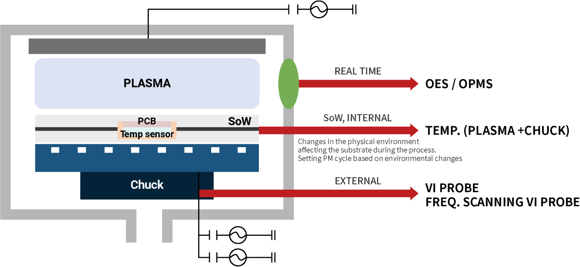
Our Sensor Wafer is used to verify the process conditions in the etching process, which is the core of the semiconductor process, and is also used in applications such as performance evaluation of etching equipment. Our sensor wafer has a size and weight similar to that of the production wafer, and is loaded into the etching equipment to monitor the temperature and plasma environment of the ESC and chamber in real time, and the result is digitized and schematized so that the operator can intuitively check the conditions. We are designed to be applicable to various test conditions from high temperature to cryogenic temperature, and are used as essential process equipment for etching equipment by providing accurate measurements for a stable test environment and actual production. In addition, we are increasing the demand and satisfaction of customers through cooperation with various equipment manufacturers.
With the development of semiconductor process technology, the precision of line width is getting more precise. In addition, the performance of etching equipment is also being advanced, and technologies such as high temperature, cryogenic temperature, various plasma environments, and EVU application are changing. In order to secure the maintenance and process stability of these equipment, the necessity of sensor wafer is emerging as an essential equipment, and in addition, technological development and cooperative development companies are required. We are developing sensor wafer that can be applied to various conditions such as high temperature, cryogenic temperature, plasma, and EUV environment, and supply products through partnerships between equipment manufacturers and semiconductor manufacturers.
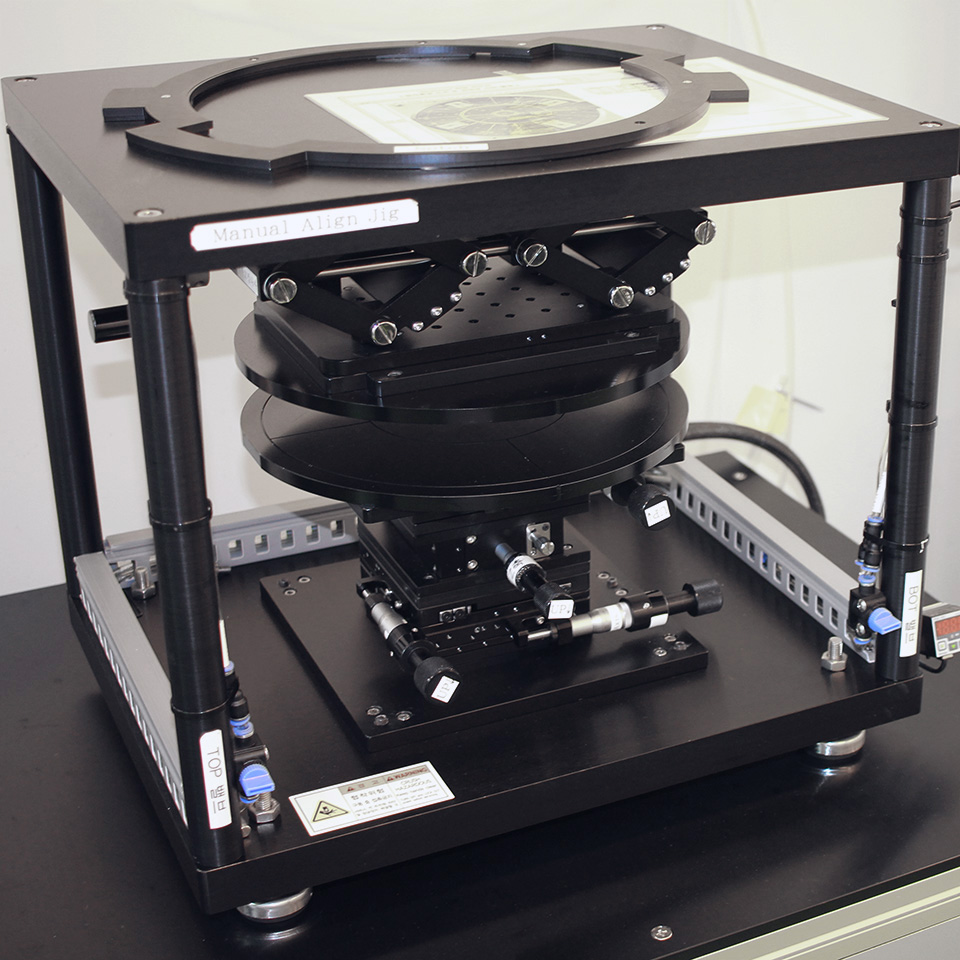
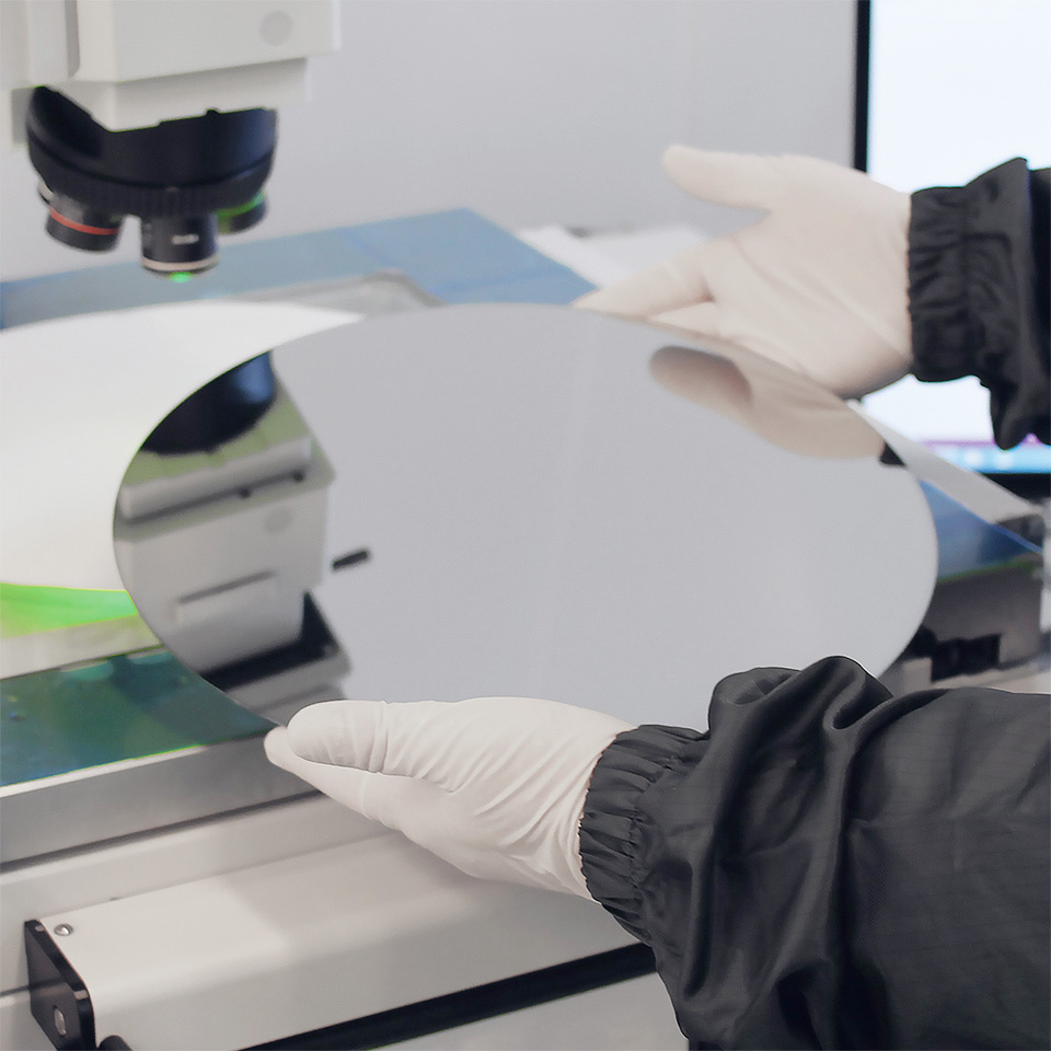
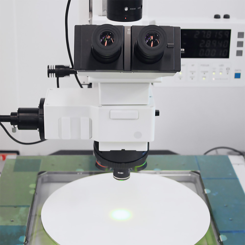
In order to secure stable measurement results and ensure uniformity, we ship products after measurement and verification in various environments. We have facilities and process equipment for related verification.
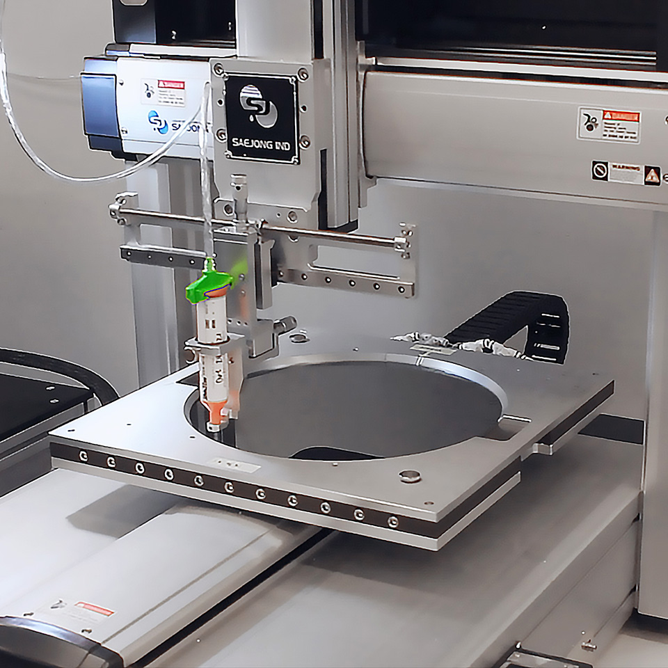
Possessing dedicated Fab facilities, equipment & analysis systems for the development and production of wafer type sensors.
Provides the best service and user experience to customers in various fields.